Product
Introduction

Laser Annealing(IGBT)
Product Inquiry
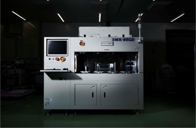
SWA-90GD
The SUMITOMO SWA-90GD is a high performance laser annealer that deposits material properties through precise heating and cooling in semiconductor and electronic device manufacturing.
- Feature
- Using a high-precision laser, the temperature of the material can be precisely controlled, optimizing the physical and electrical properties of the material
- The high processing speed allows it to be used efficiently in high volume production environments, significantly increasing productivity
- The laser intensity and position can be precisely adjusted to ensure uniform heating of the material surface, delivering high quality results
- Used for a wide range of materials and applications, including semiconductor wafers, display panels, solar cells and more
- The intuitive user interface and high level of automation reduce operator fatigue and increase work efficiency
Detailed Specification
Green Laser Annealing
Laser annealing is a process in which a laser is used to rapidly and precisely heat a specific area of a material, followed by rapid cooling.
This technique is widely used in the semiconductor industry to improve the electrical properties of materials by controlling impurity diffusion and recrystallisation.
SWA-90GD
It is a high performance laser annealer capable of deep activation and double pulse processing.
The energy stable, maintenance free and compact design of the system contributes to the development of next generation semiconductor processes.
- Deep activation
- Activation up to 7μm is possible.
- High pulse energy stability
- Equipped with energy feedback function. Achieved in-plane uniformity σ<=1%.
- Double pulse control further controls temperature distribution and time in the depth direction
- Optimization of annealing process is possible even under temperature constraints.
- Maintenance-free solid-state laser enables production at high operating rates
- Compared to gas lasers, running costs can be significantly reduced.
- Compact laser oscillator
- It is possible to save space in the equipment installation area.
- 70μmt thin wafer transfer