Product
Introduction

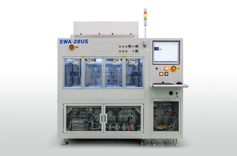
SWA-20US
The SUMITOMO SWA-20US is a high performance laser annealer for precise temperature control and high-speed processing in semiconductor and electronic device manufacturing.
- Feature
- Precise control of the laser allows only specific parts of the material to be heated, minimizing thermal damage
- Laser heating and cooling is extremely fast, reducing the overall process time
- The high temperature treatment improves the crystal structure and enhances the time and physical properties of the material
- The intensity, position and time of the laser can be precisely controlled to achieve highly consistent results
- The laser operates in a non-contact manner, allowing processing without mechanical stress or contamination
Detailed Specification
UV Laser Annealing
Laser annealing is a process in which a laser is used to rapidly and precisely heat a specific area of a material, followed by rapid cooling.
This technique is widely used in the semiconductor industry to improve the electrical properties of materials by controlling impurity diffusion and recrystallisation.
SWA-20US
Laser anneal system for next generation power device.
It is used to create and activate SIC ohmic contacts.
By suppressing the temperature rise of the non-irradiated surface and heating
the metal-SIC interface to a high temperature, OPTSWING creates an O’mic contact.
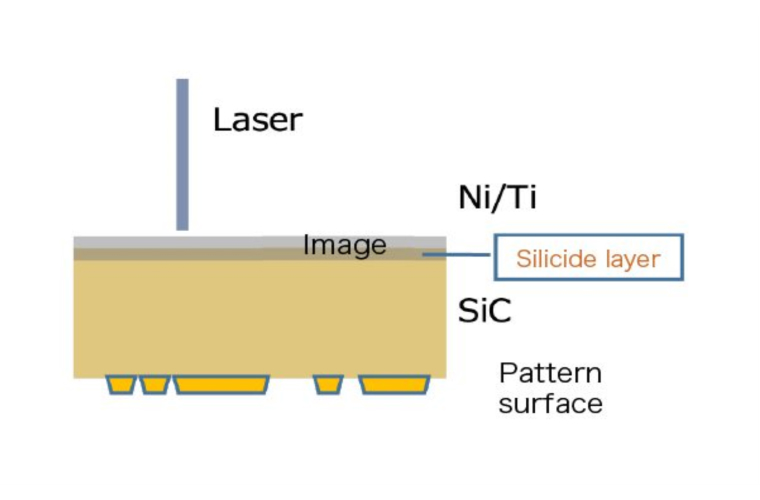
Annealing of the SIC wafer is used to silicide the backside electrode.
*Note: In Si-IGBT, it is widely used to activate impurities injected on the backside.